Fabrication
Detailed Protocol
Microfluidic Chips Production
Work done by Yu Zhenming (sophomore) with the help of Chen Rifei (junior). Assistant professor Jaewon Park, docter Wang Yao and docter Zhang Rui have offered their advices.
After reading existing papers about the processing technology typically used in microfluidic chips production and endless trial experiment, we have formed our own processing protocol based on our equipment.
The microfluidic chips used in our project were all produced using this protocol.
Process Overview
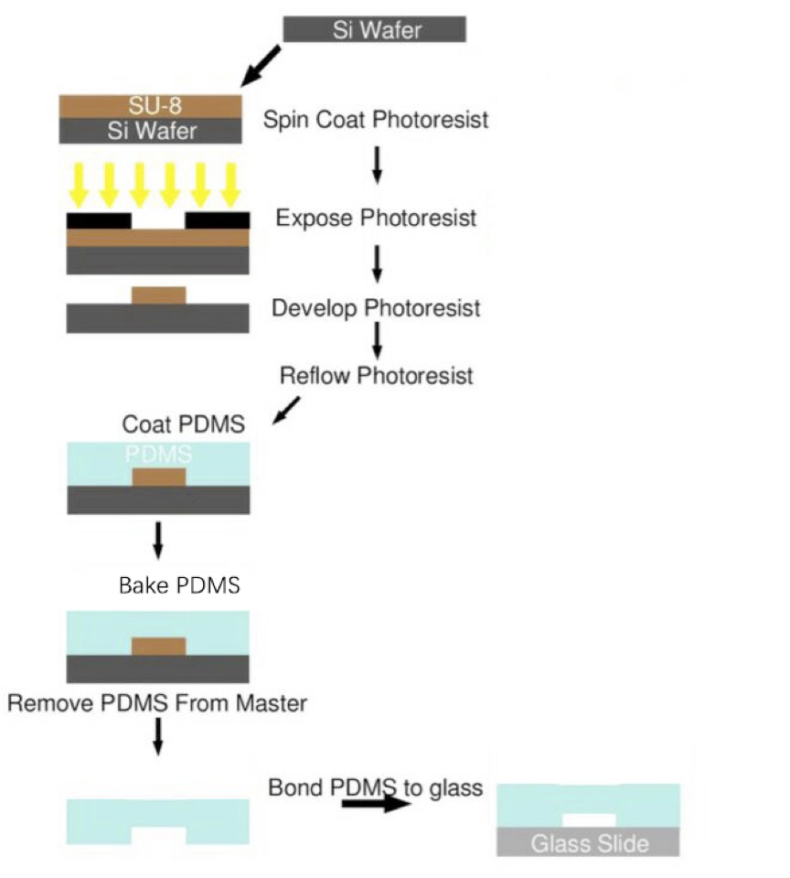
SU-8 Photoresist can cross-link to a network of polymer when exposed to short wavelength light. If the cross-linked network has formed, it cannot be dissolved by the SU-8 developer. So if we place a photo mask to shade the light shine on the photoresist, we can make a copy of the pattern on the photo mask.
Both PDMS and glass contains silicon element. When they were treated by oxygen plasma, unstable hydroxyl group will form on the treated surface. When they get close enough, two hydroxyl group will dehydrate and bond together covalently.
Detailed Protocol
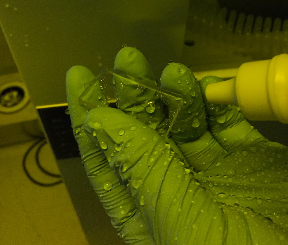
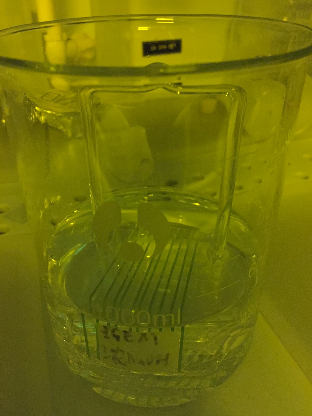
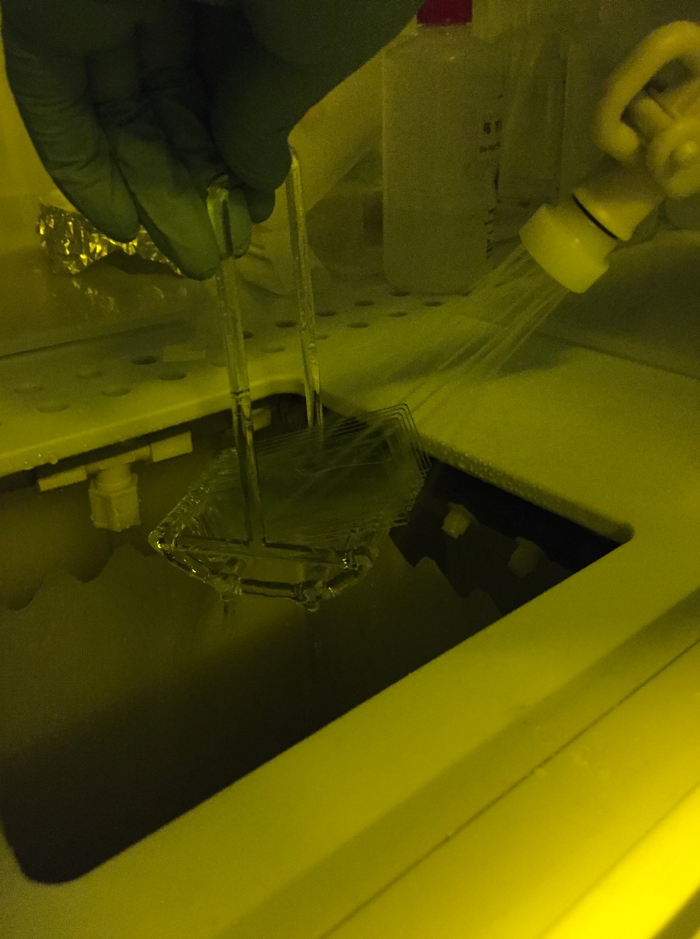
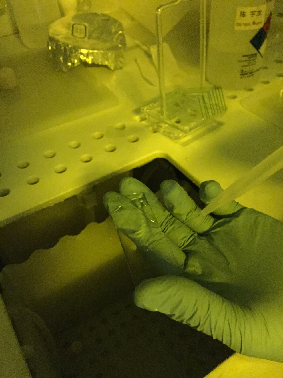
- Wash the glass mask holder by socking it in dilute ammonia water for over 1 hour, and refresh it with deionized water.
- Wash the glass mask holder by socking it in dilute hydrochloric acid for over 1 hour, and refresh it with deionized water.
- Wash the glass mask holder by socking it in positive photoresist remover for over 1 hour, and refresh it with deionized water.
- Dry the glass mask holder in the drying oven.
- Clean the mask film by wiping the two sides carefully on one direction with a clean paper socked in acetone.
- Clean the mask for the second time film by wiping the two sides carefully on one direction with a clean paper socked in alcohol or isopropyl alcohol.
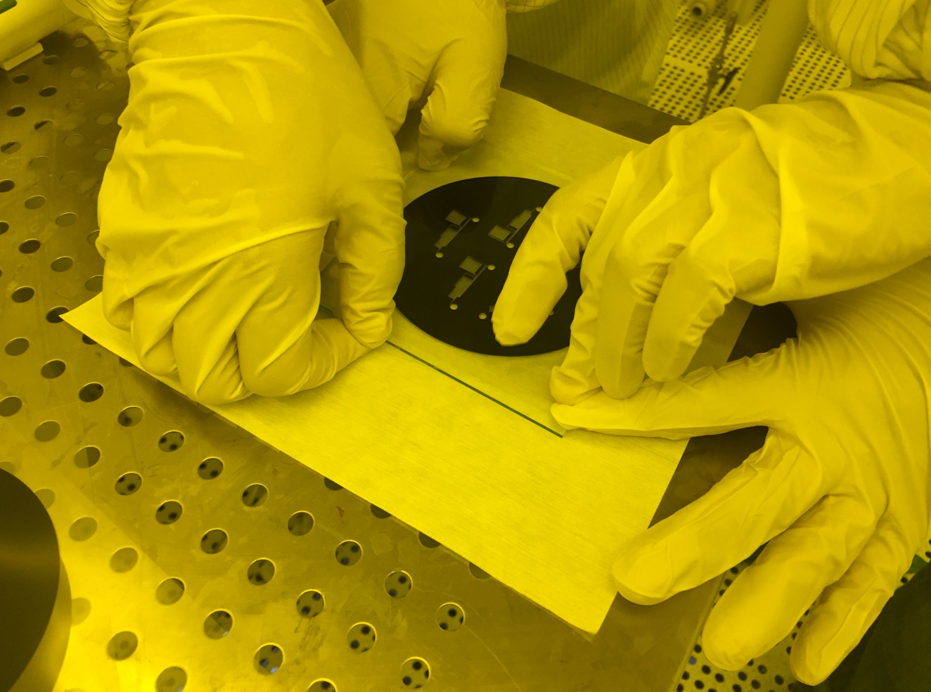
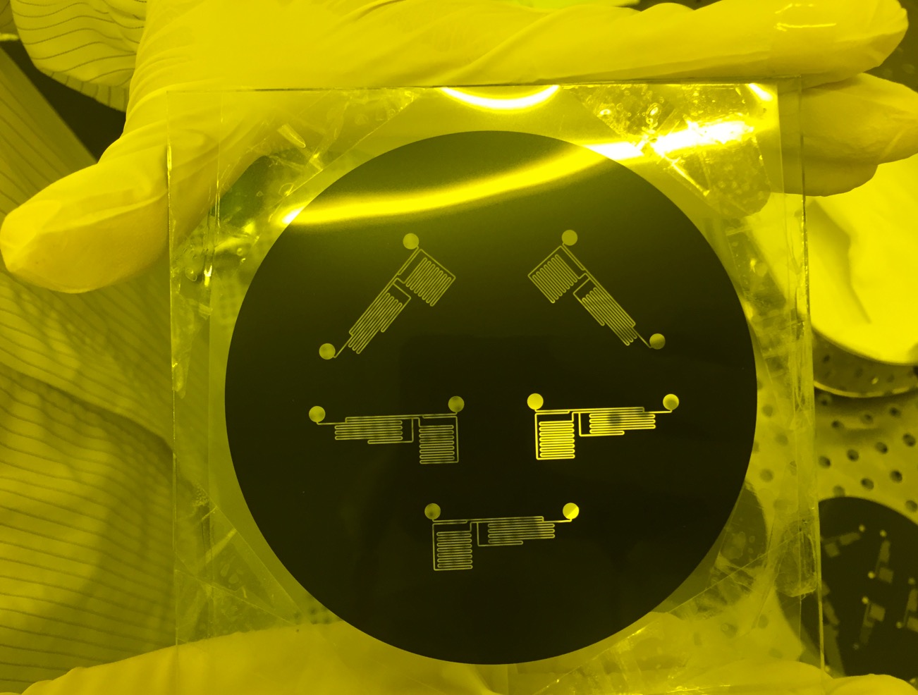
- Fix the mask film on to the mask holder with tape.
- The tape can only touch the edges of the mask film in order to prevent contamination.
- Pour some SU-8 2100 photoresist in a small bottle, keep it still in the refrigerator for at least a week(two weeks recommend) to remove the bobbles inside the photoresist.
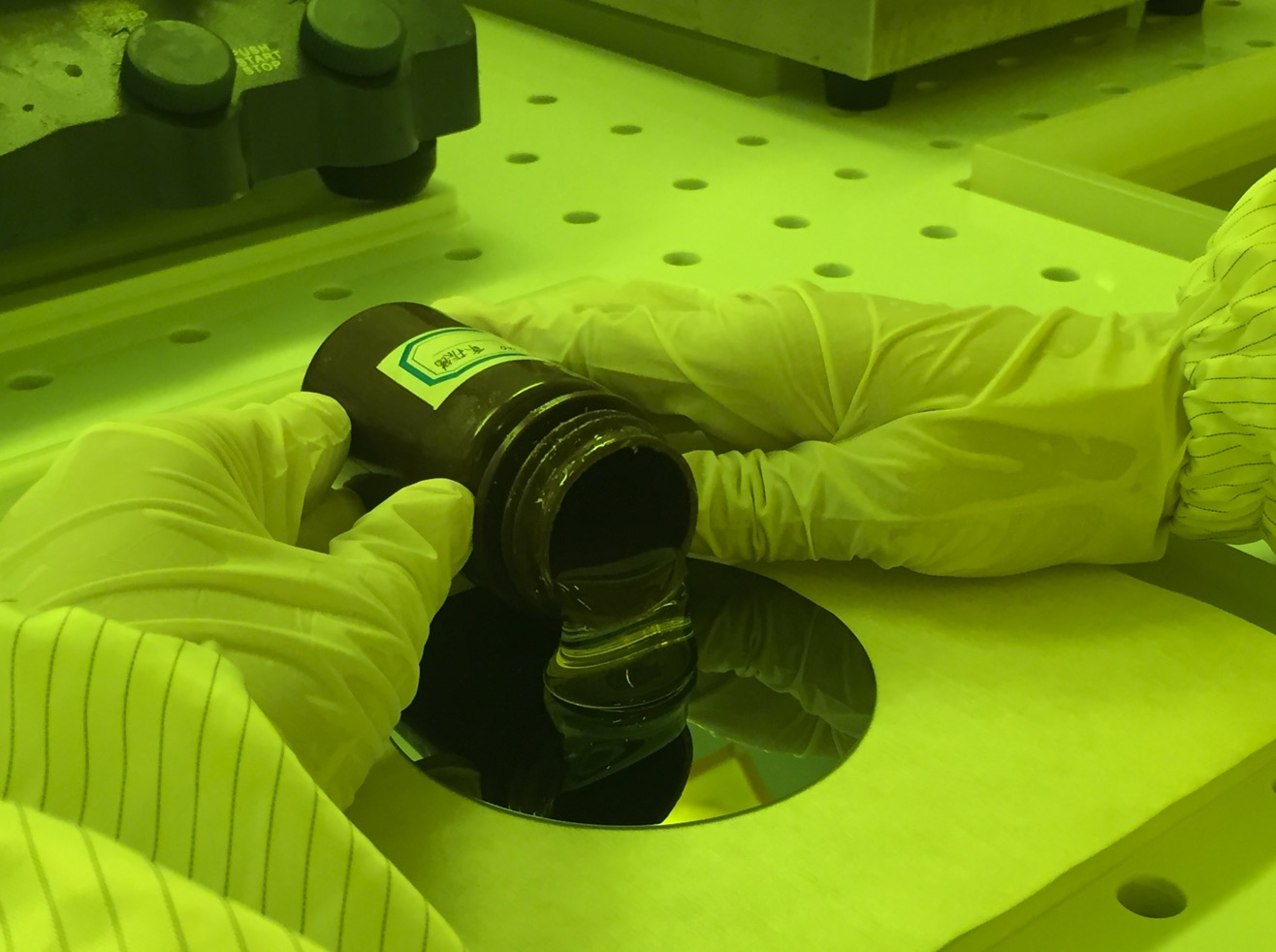
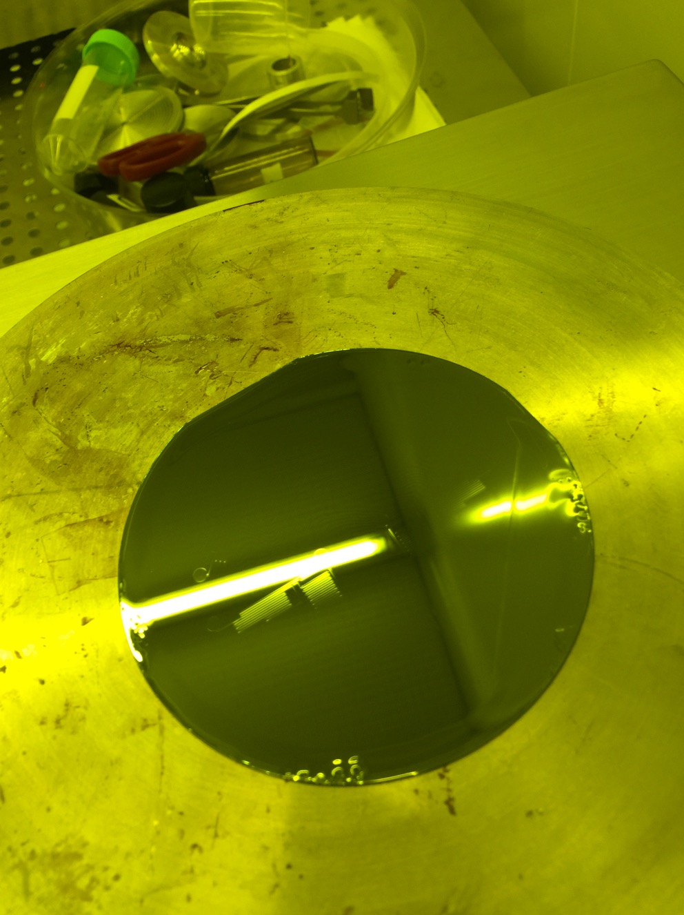
- Take the SU-8 photoresist out from the refrigerator, wait until the bottle hit room temperature, and carefully pour it on to a clean silicon wafer. The bottle should be held as close to the wafer as possible to prevent bobble from generating.
- Spin the wafer with photoresist on the spin coater with the following procedure.
- Spin at 500 rpm for 10 seconds with acceleration time of 5 seconds.
- Spin at 2000 rpm for 30 seconds with acceleration time of 5 seconds.
- Spin at 500 rpm for 5 seconds with acceleration time of 5 seconds.
- Stop with acceleration time of 5 seconds.
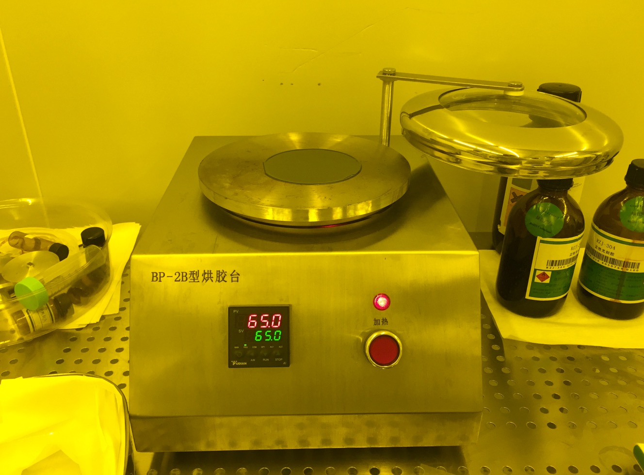
- Bake the wafer on 65℃ hotplate for 5 minutes.
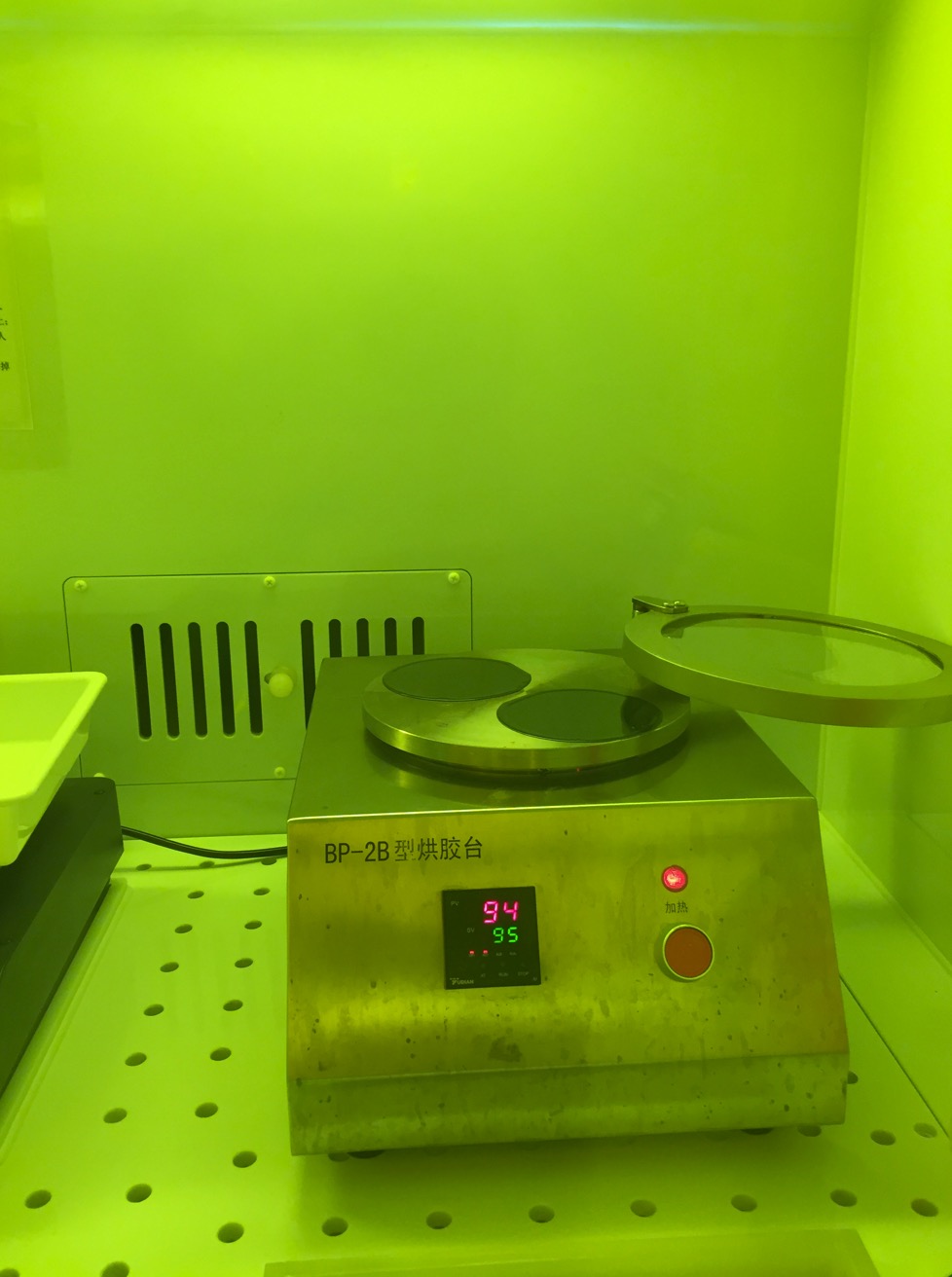
- Bake the wafer on 95℃ hotplate for 30 minutes.
- Keep the wafer still in room temperature for more than 1 hour and wait until the photoresist is dry enough.
- Clean the backside of the wafer with a clean paper socked in SU-8 developer to remove excessive photoresist.
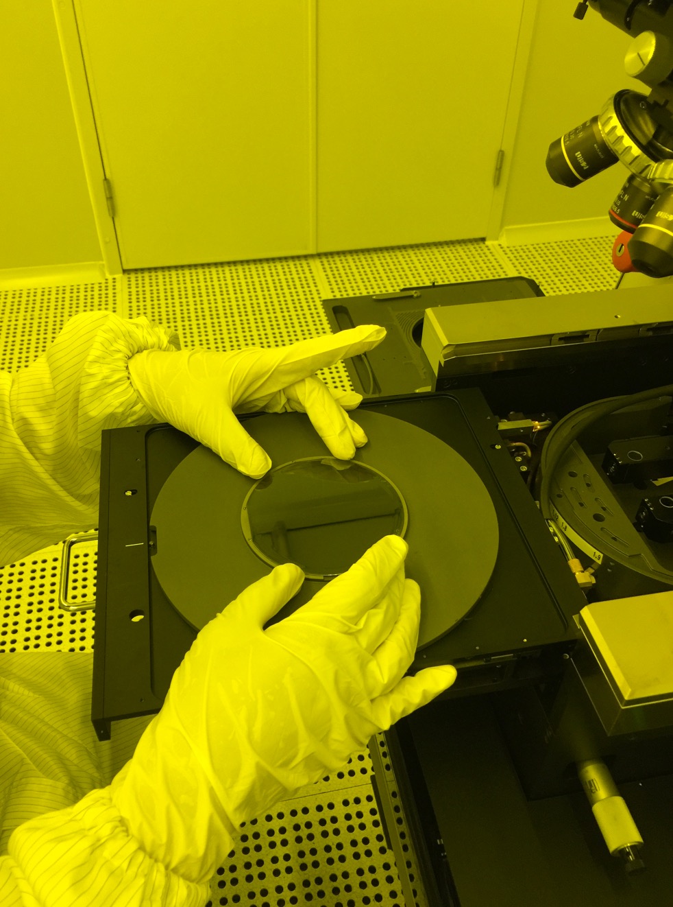
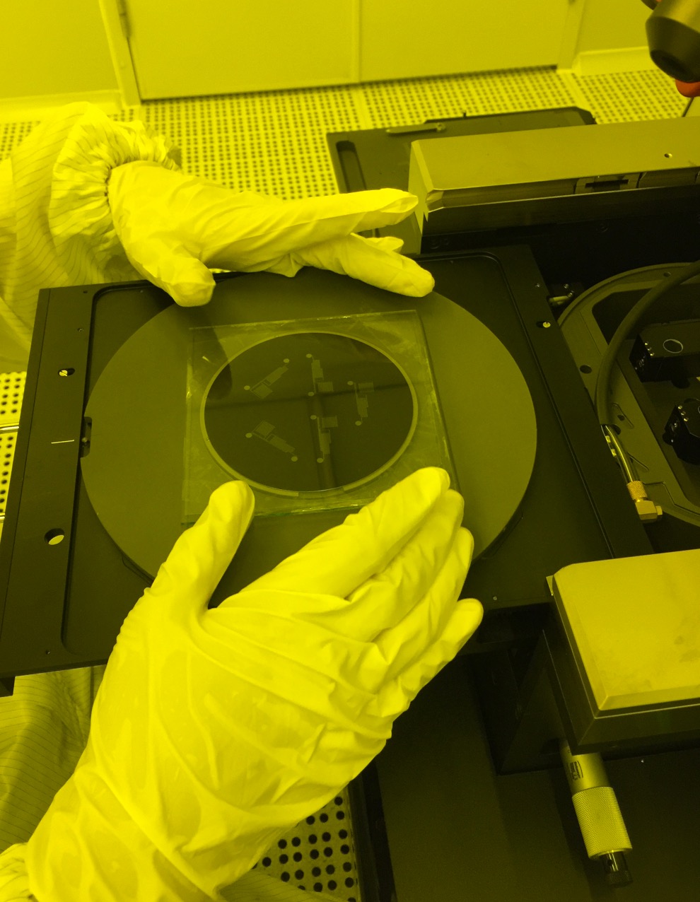
- Fix the wafer to the mask aligner.
- Place the mask holder on the wafer carefully.
- Expose the wafer with the mask aligner with the exposure energy of 220 mJ/cm2.
- Bake the wafer on 65℃ hot plate for 5 minutes.
- A visible pattern identical to the photomask will be seen in the film within 5 seconds after being placed on the hotplate.
- Bake the wafer on 95℃ hot plate for 12 minutes.
- Keep the wafer still in room temperature for 15 minutes and wait until the photoresist is dry enough.
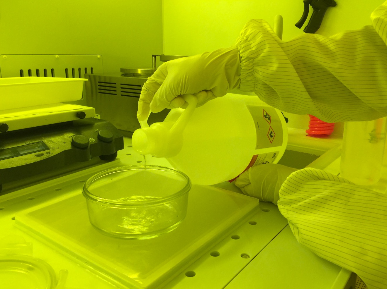
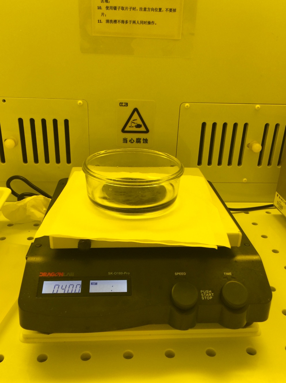
- Pour fresh SU-8 developer into the container. Place the container on the shaking table and set the speed to 400rpm. Start the shaking table and wait for the speed to be stabilized.
- Put the wafer in the container and develop for 4 minutes.
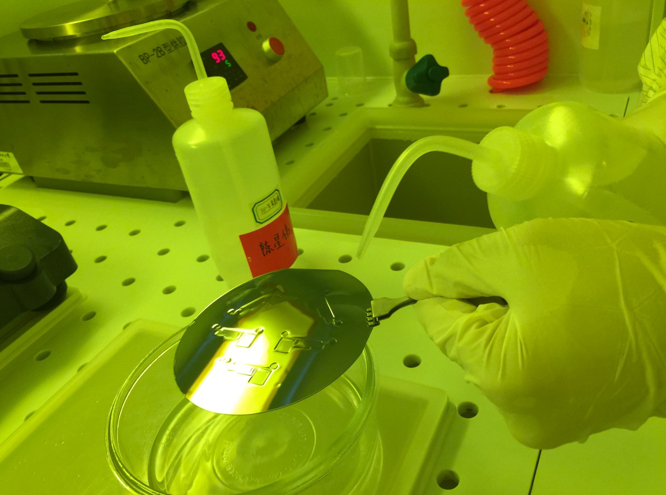
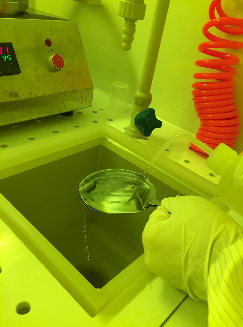
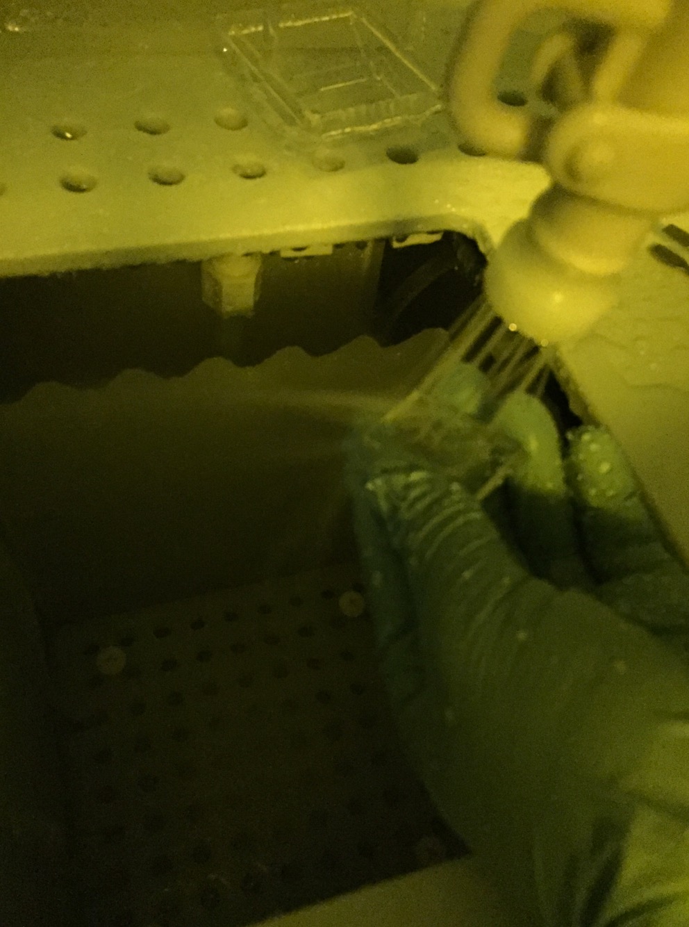
- Spray and wash the developed image with fresh developer for approximately 10 seconds.
- Spray and wash the developed image with isopropyl alcohol for approximately 10 seconds.
- Air dry the wafer with nitrogen gun.
- Bake the wafer on 150℃ hot plate for 20 minutes.
- Check the developed image.
- Wait for the wafer to cool down.
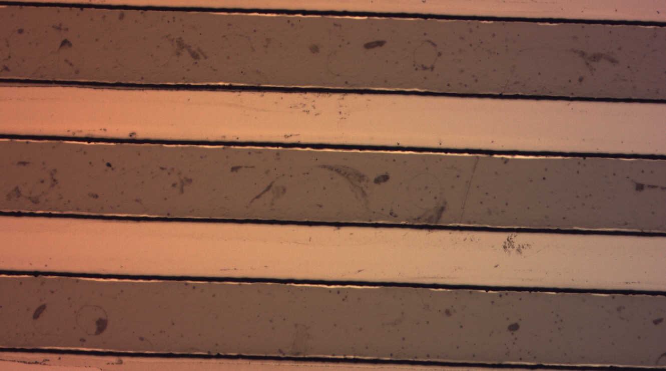
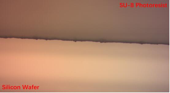
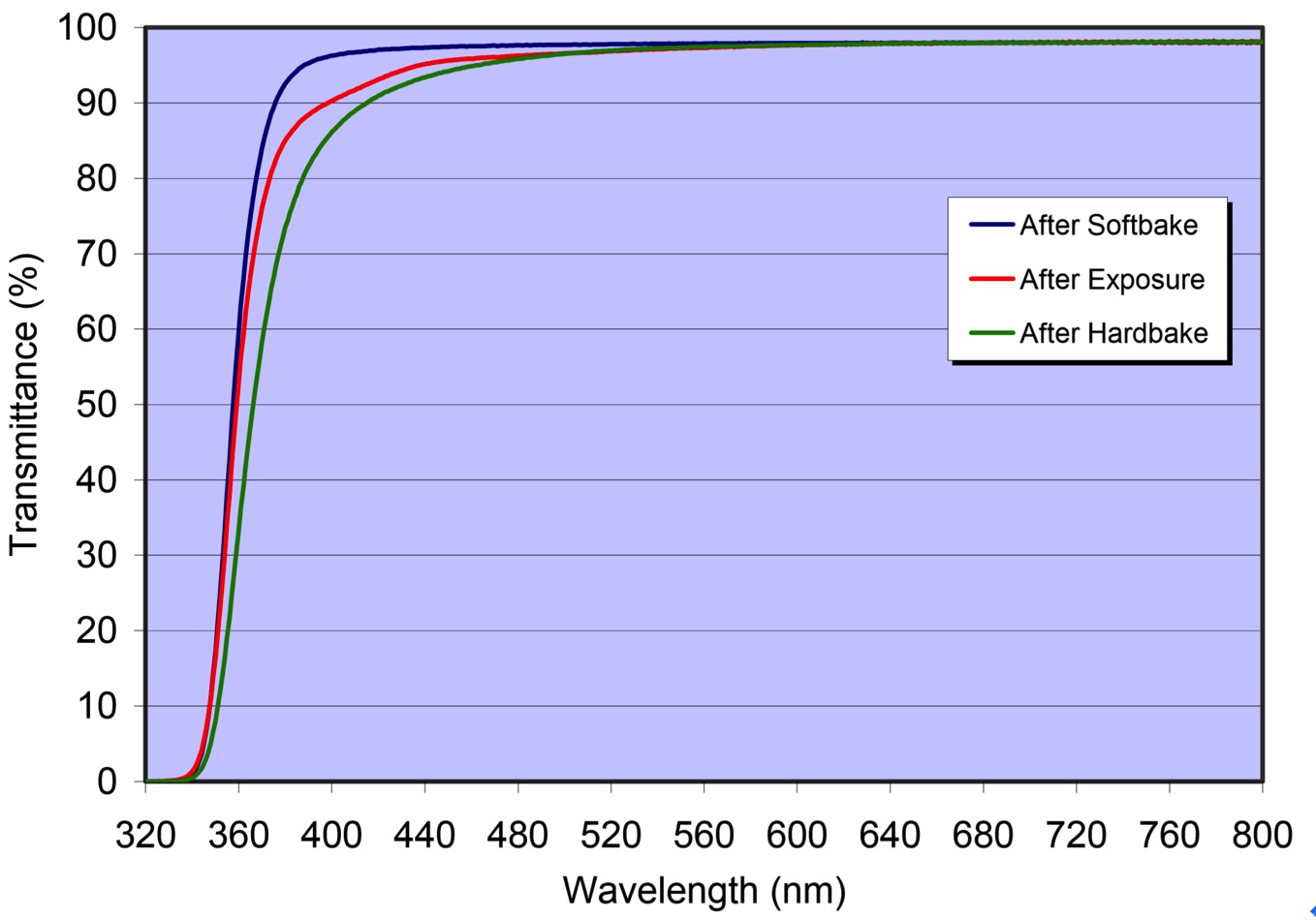
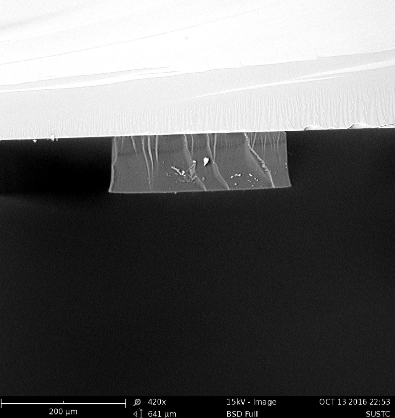
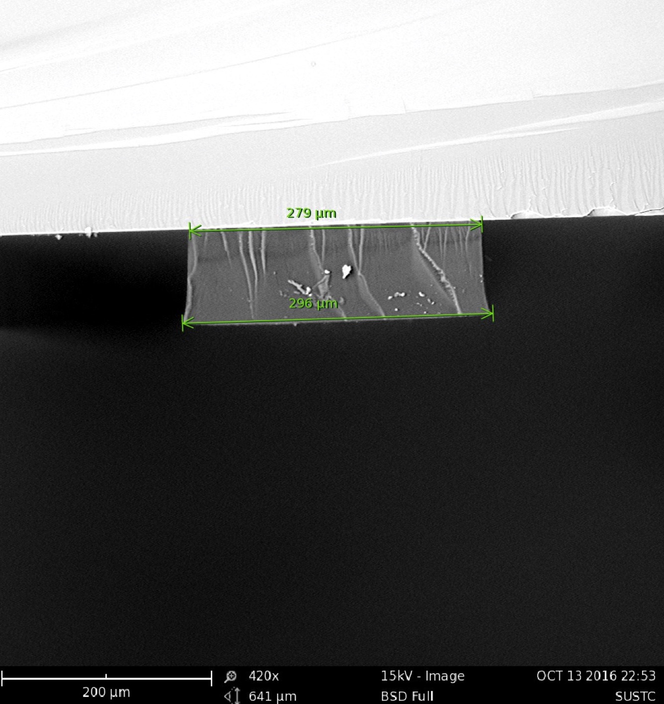
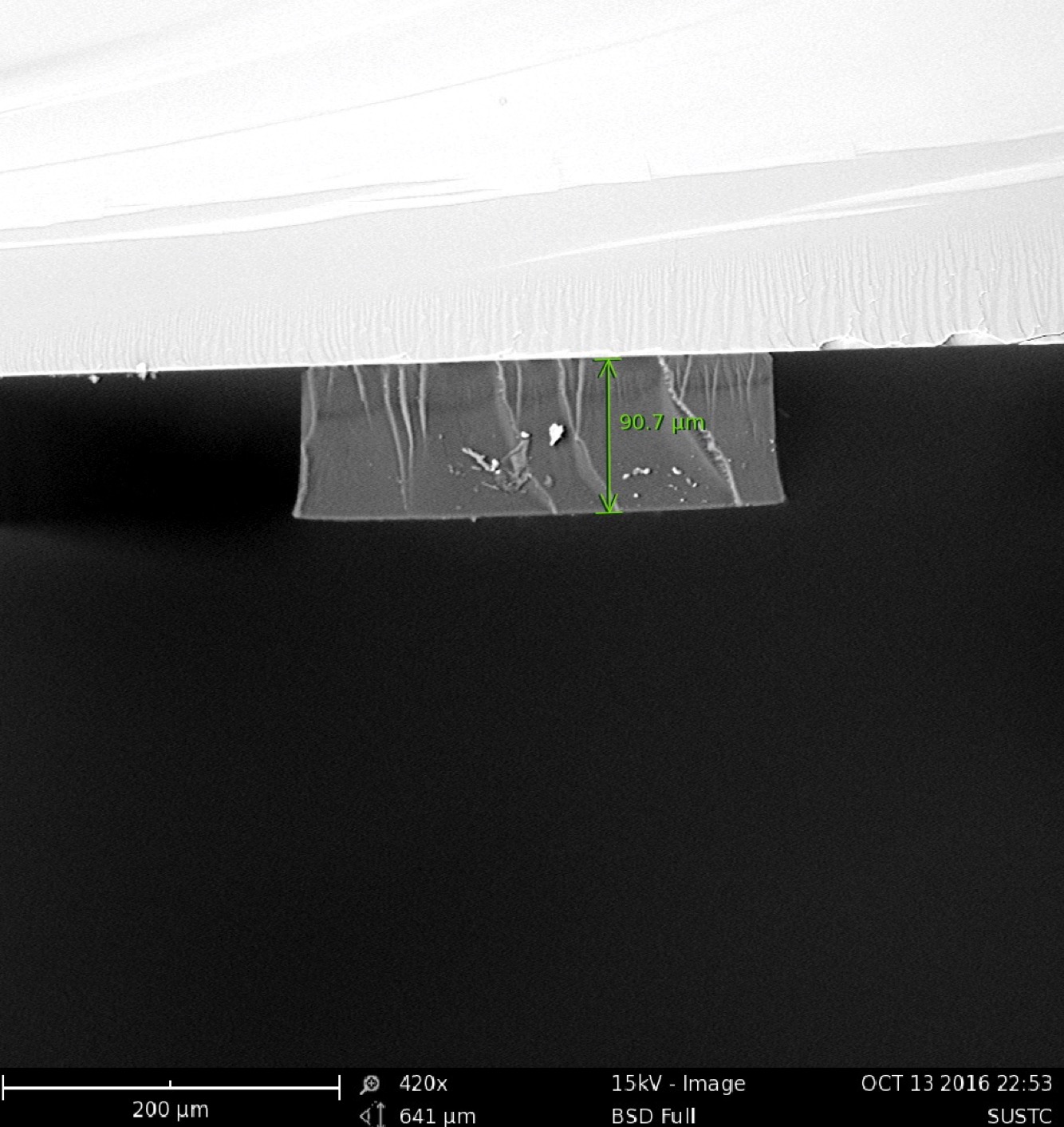
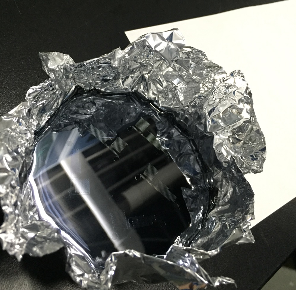
- Check the final image of the photoresist. The final image usually has a lot of defects at the edges of the channels. And due to the low transmittance of SU-8 photoresist to the low-wavelength light, the photoresist at the top side of the channel will absorb higher energy than the photoresist at the bottom, causing a trapezoidal cross section profile.
- Mix about 30g PDMS base with about 3g curing agent (at the ratio of 10:1).
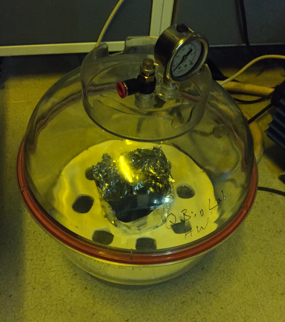
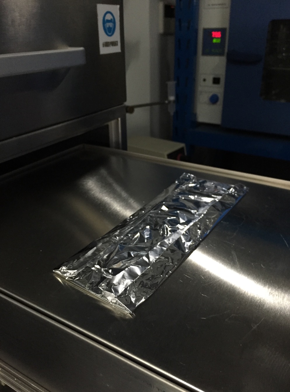
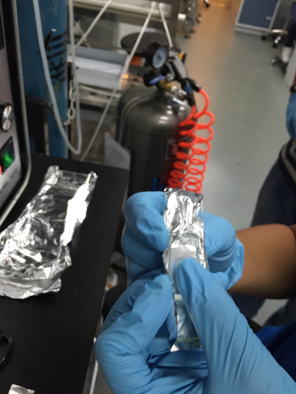
- Wrap the wafer with tinfoil and pour the PDMS mix on to the wafer.
- Put the wafer in the vacuum dryer to remove the bobbles inside.
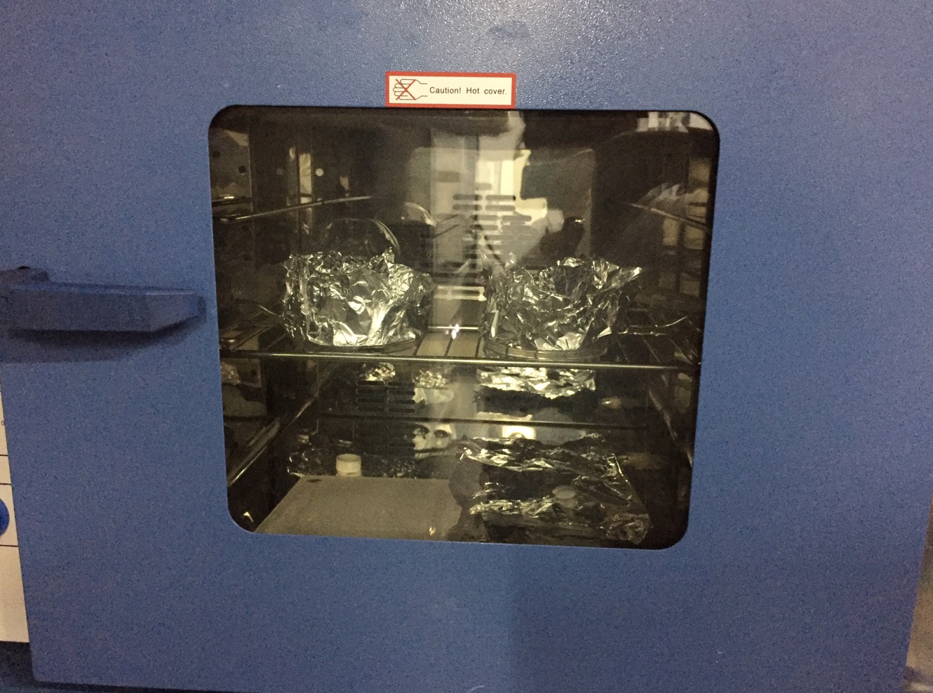
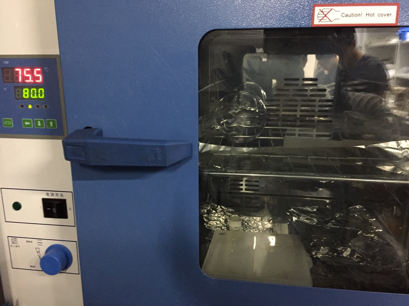
- Bake the wafer in the 80℃ drying oven for 3 hours.
- Take the wafer out and rip off the tinfoil.
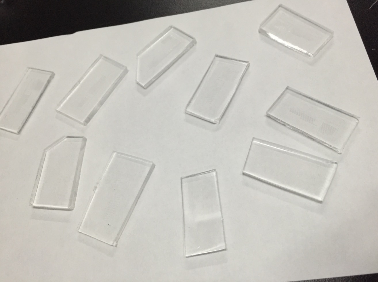
- Carefully remove PDMS from the wafer and cut it into pieces on a piece of clean paper.
- Spray and wash the PDMS with alcohol.
- Spray and wash the PDMS with deionized water.
- Air dry the wafer with nitrogen gun.
- Soak glass slides in 100g/L NaOH solution for 14~24 hours.
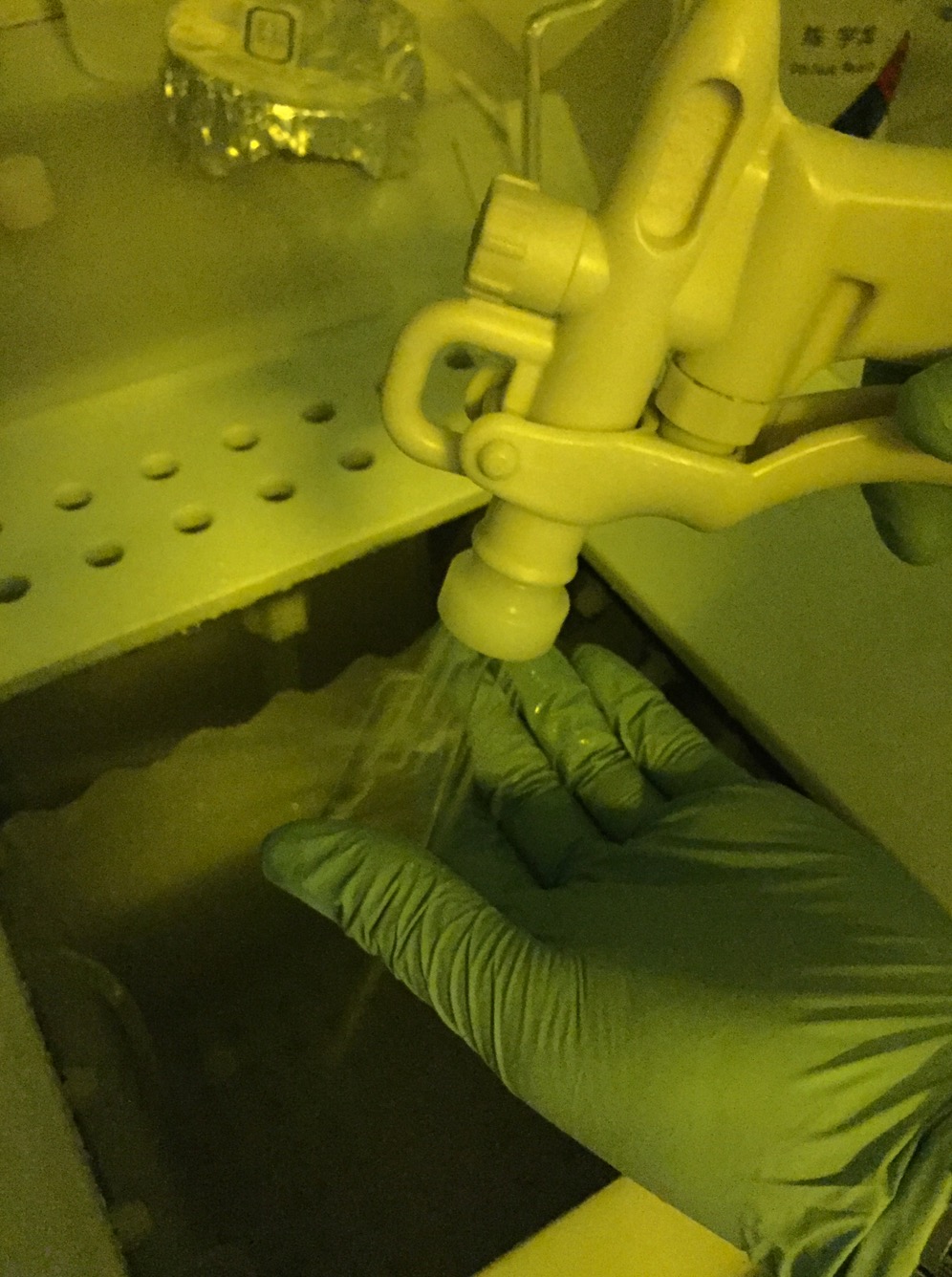
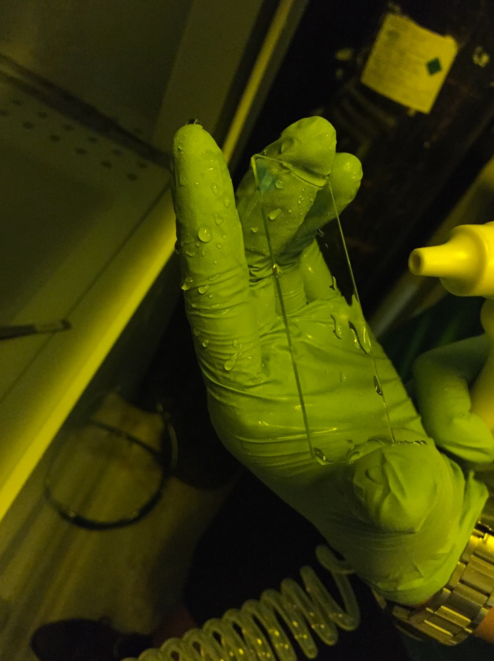
- Take the glass slides out, spray and wash them with deionized water.
- Spray and wash the glass slides with alcohol.
- Spray and wash the glass slides with deionized water.
- Air dry the wafer with nitrogen gun.
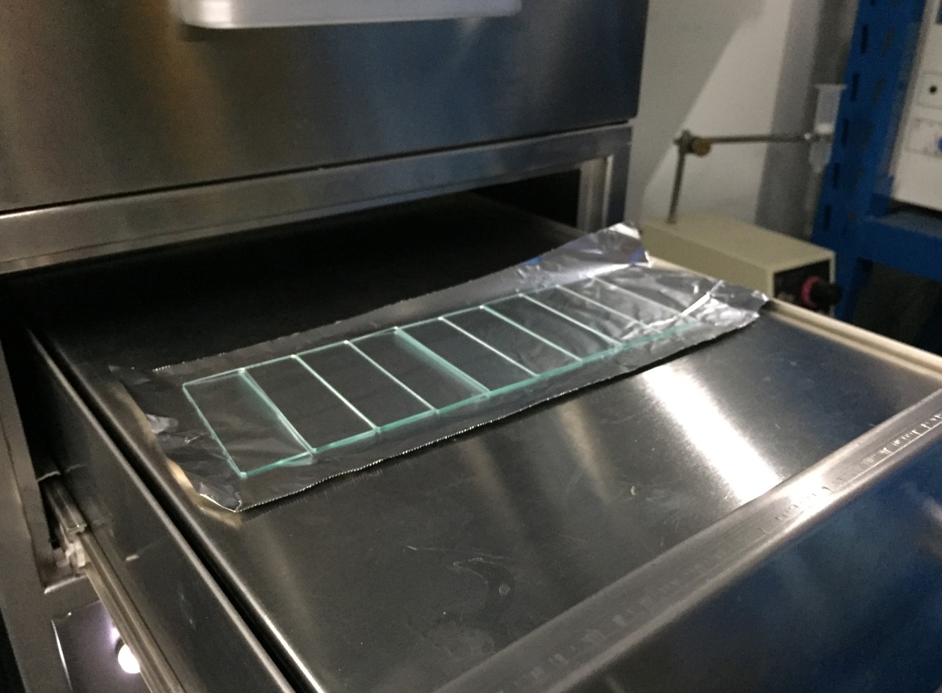
- Place the clean slides on a piece of tinfoil.
- Dry the glass slides in the drying oven
- Clean the glass slide in the ultra-violet ozone cleaner for 15 minutes.
- Take the slides out and wrap them with another piece of tinfoil.
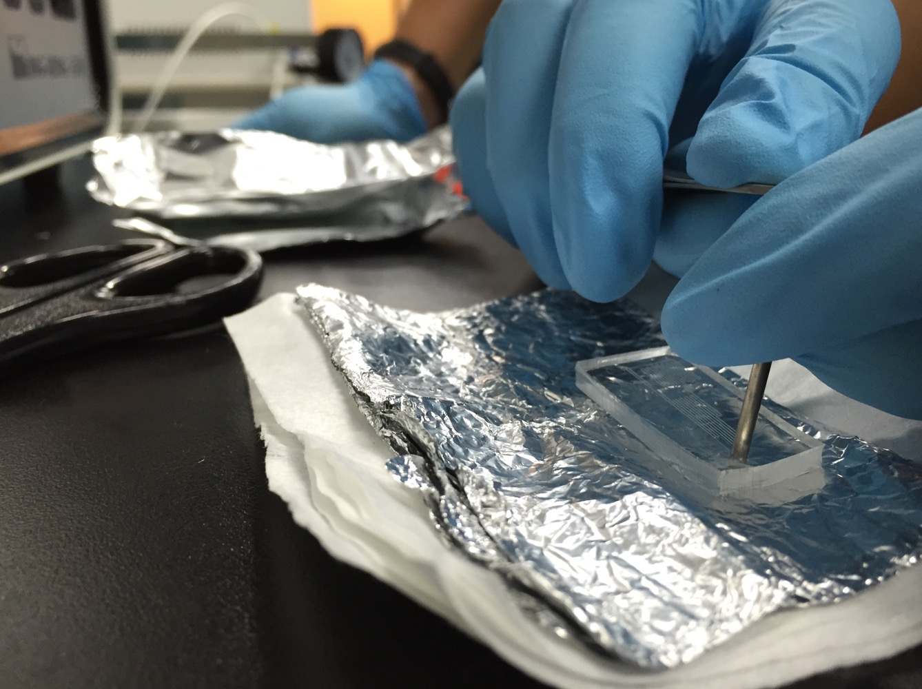
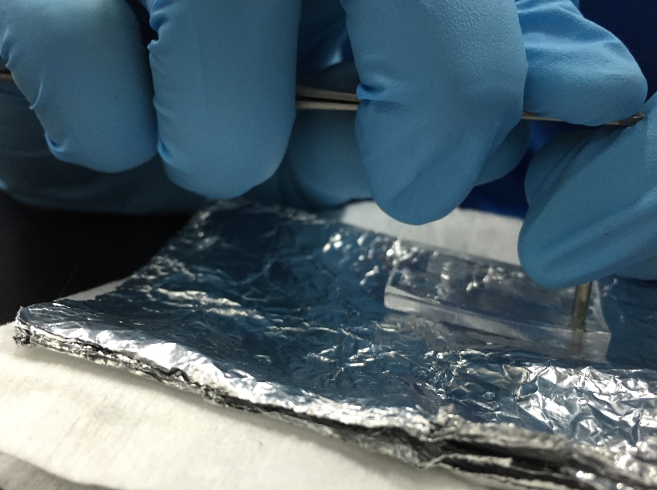
- Punch the holes for the tube on the PDMS.
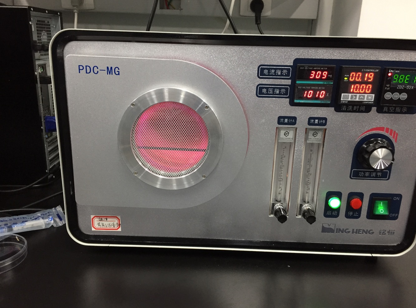
- Open the plasma cleaner and place the PDMS and the slide in the meddle. A piece of tinfoil should be placed under the PDMS.
- Treat them with oxygen plasma for 1.5 minutes at 300W and the oxygen flow rate of 0.6mL/min.
- Stop the plasma cleaner and open the cover as soon as possible. Press the treated sides together and apply pressure within 5 seconds.

