| Line 158: | Line 158: | ||
Both PDMS and glass contains silicon element. When they were treated by oxygen plasma, unstable hydroxyl group will form on the treated surface. When they get close enough, two hydroxyl group will dehydrate and bond together covalently. | Both PDMS and glass contains silicon element. When they were treated by oxygen plasma, unstable hydroxyl group will form on the treated surface. When they get close enough, two hydroxyl group will dehydrate and bond together covalently. | ||
| − | + | <html><a href="/Team:SUSTech_Shenzhen/Notebook/Fabrication" class="btn">Detailed Protocol</a></html> | |
| − | + | ||
| − | + | ||
| − | + | ||
| − | + | ||
| − | + | ||
| − | + | ||
| − | + | ||
| − | + | ||
| − | + | ||
| − | + | ||
| − | + | ||
| − | + | ||
| − | + | ||
| − | + | ||
| − | + | ||
| − | + | ||
| − | + | ||
| − | + | ||
| − | + | ||
| − | < | + | |
| − | < | + | |
| − | + | ||
| − | + | ||
| − | + | ||
| − | + | ||
| − | + | ||
| − | + | ||
| − | + | ||
| − | + | ||
| − | + | ||
| − | + | ||
| − | + | ||
| − | + | ||
| − | + | ||
| − | + | ||
| − | + | ||
| − | + | ||
| − | + | ||
| − | + | ||
| − | + | ||
| − | + | ||
| − | + | ||
| − | + | ||
| − | + | ||
| − | + | ||
| − | + | ||
| − | + | ||
| − | + | ||
| − | + | ||
| − | + | ||
| − | + | ||
| − | + | ||
| − | + | ||
| − | + | ||
| − | + | ||
| − | + | ||
| − | + | ||
| − | + | ||
| − | + | ||
| − | + | ||
| − | + | ||
| − | + | ||
| − | + | ||
| − | + | ||
| − | + | ||
| − | + | ||
| − | + | ||
| − | + | ||
| − | + | ||
| − | + | ||
| − | </ | + | |
| − | + | ||
| − | + | ||
| − | + | ||
| − | + | ||
| − | + | ||
| − | + | ||
| − | + | ||
| − | + | ||
| − | + | ||
| − | + | ||
| − | + | ||
| − | + | ||
| − | + | ||
| − | + | ||
| − | + | ||
| − | + | ||
| − | + | ||
| − | + | ||
| − | + | ||
| − | + | ||
| − | + | ||
| − | + | ||
| − | + | ||
| − | + | ||
| − | + | ||
| − | + | ||
| − | + | ||
| − | + | ||
| − | + | ||
| − | + | ||
| − | + | ||
| − | + | ||
| − | + | ||
| − | + | ||
| − | + | ||
| − | + | ||
| − | + | ||
| − | + | ||
| − | + | ||
| − | + | ||
| − | + | ||
| − | + | ||
| − | + | ||
| − | + | ||
| − | + | ||
| − | + | ||
| − | + | ||
| − | + | ||
| − | + | ||
| − | + | ||
| − | + | ||
| − | + | ||
| − | + | ||
| − | + | ||
| − | + | ||
| − | + | ||
| − | + | ||
| − | + | ||
| − | + | ||
| − | + | ||
| − | + | ||
| − | + | ||
| − | + | ||
| − | + | ||
| − | + | ||
| − | + | ||
| − | + | ||
| − | + | ||
| − | + | ||
| − | + | ||
| − | + | ||
| − | + | ||
| − | + | ||
| − | + | ||
| − | + | ||
| − | + | ||
| − | + | ||
| − | + | ||
| − | + | ||
| − | + | ||
| − | + | ||
| − | + | ||
| − | + | ||
| − | + | ||
| − | + | ||
| − | + | ||
| − | + | ||
| − | + | ||
| − | + | ||
| − | + | ||
| − | + | ||
| − | + | ||
| − | + | ||
| − | + | ||
| − | + | ||
| − | + | ||
| − | + | ||
| − | + | ||
| − | + | ||
| − | + | ||
| − | + | ||
| − | + | ||
| − | + | ||
| − | + | ||
| − | + | ||
| − | + | ||
| − | + | ||
| − | + | ||
| − | + | ||
| − | + | ||
| − | + | ||
| − | + | ||
| − | + | ||
| − | + | ||
| − | + | ||
| − | + | ||
| − | + | ||
| − | + | ||
| − | + | ||
| − | + | ||
| − | + | ||
| − | + | ||
| − | + | ||
| − | + | ||
| − | + | ||
| − | + | ||
| − | + | ||
| − | + | ||
| − | + | ||
| − | + | ||
| − | + | ||
| − | + | ||
| − | + | ||
{{:Team:SUSTech_Shenzhen/main-content-end}} | {{:Team:SUSTech_Shenzhen/main-content-end}} | ||
{{:Team:SUSTech_Shenzhen/wiki-footer}} | {{:Team:SUSTech_Shenzhen/wiki-footer}} | ||
{{:Team:SUSTech_Shenzhen/themeJs}} | {{:Team:SUSTech_Shenzhen/themeJs}} | ||
Revision as of 11:54, 17 October 2016

Hardware
Model
Contents
Introduction
We are aiming to evolve a more sensitive mechanical sensitive channel (MS channel). When MS channels are stimulated by mechanical force, a Ca2+ influx is triggered. To measure the performance of MS channel, we chose sound to produce mechanical force and GECO protein as Ca2+ indicator to reflect the channel sensitivity through its fluorescence change.
Sound part
In this part, we aim to explore the effect different frequency on the cells. Frequencies from 300Hz to 1.7MHz were tried to observe whether the cells with MS channel can response differently to different frequency. If so, frequency orthogonal audiogenetic parts are hopefully to be developed. Meanwhile, the equipment was also designed to be easy to change sonic power, in order to choose the most suitable intensity being harmless to the cells.
Sonic Stimulation
Signal generation
A dual channel function/arbitrary waveform generator (Feel Tech FY2303) was used to generate sound wave signals. It can generate 1uHz to 2MHz, 0v to 20v signals. An amplifier was used to amplify the wave signal output by the wave generator.Sound generator
Buzzer
Buzzer is a thin metal plate attached with a piezoelectric ceramic. When varying voltage is added to its two ends, it deforms coordinately. Whereas, its low and high frequency response is weak, and can only be used to generate sound under 15 KHz. For the safety of the cells, we fix it on the bottom of cell dish for cellular stimulation.Speaker
As the low and high frequency response of buzzer is weak, speaker (Type: rsiym) was chose for complementation. Its power can reach 3W and it was drenched in culture medium for low frequency experiment.Balanced Amateur
Buzzers and speakers both have short comes. For buzzers, sound could mainly be absorbed by cell dish bottom and the power was very weak. Speaker is more powerful though, it is cell toxic and not stable. For more, they both apply normal stress to the cells rather than shear stress. So, we promoted a third plan using balanced amateur.
Balanced amateur is very stable and small. A steel tube was fixed on it to drench in to water. Thus it can generate a shear force horizontal to cell dish, which is closer to the mechanism of human hearing. The problem is that its power is not strong enough to trigger a cellular response.
Lab Circuit
The following is a brief circuit of sound generator circuit.
ultra sound stimulation
Seeing cellular response increased with stimulating frequency, and hearable sound can hardly trigger strong cellular response. Ultrasound was come up with. There were 4 kinds of ultrasound devices constructed.
Horn-shaped ultrasound generator
We first constructed this device using circuits from ultrasound cleaner. However it was easy to destroy the circuit due to too small load.
Piezoelectric Energy Transducer.
A new ultrasound device was designed seeing the horn-shaped device is too powerful and unstable. Piezoelectric energy transducer was chose for a much slighter stimulation.
Ultrasound signal generator:
KINGCHIP SD02-JSQ-V2.4 circuit, 5V DC input. 1.7MHz output.
Power control:
The signal output from KINGCHIP SD02-JSQ-V2.4 circuit was input to the following conrol circuit designed by ourselves. Output power can be controled by changing resistance. Microproccsor Arduino UNO was rogrammed to control stimulation time pattern.
Energy Transducer:
1. 1MHz energy transducer used in fog generator was used to generate stable ultrasound. Cell toxity experiment show that it has little and tolerable cell toxity.
2. For quantified stimulation, a calibrated ultrasound energy transducer was used.
Data
Diameter: 8.5mm
Thinness: 22mm
For 23Vp-p 1MHz input, 1.9W/cm2 (3mm for from head)
Lab Circuit
Device I
Two 1MHz low power ultrasound stimulators are implemented for program controlled exeriment.
Device II
One 1MHz ultrasound stimulator was implemented with larger size and maximun power. Control part and electric part were seperated into two layers for safety.
1. Stimulation program loading.
2. Fix stimulator in proper position.
3. Turn on the switch and change resistance for proper ultrasound intensity.
4. Start stimulation experimrnt.
Microfluidics
Why Microfluidics
Microfluidics is a multidisciplinary field intersecting engineering, physics, chemistry, biochemistry, nanotechnology, and biotechnology, with practical applications in the design of systems in which low volumes of fluids are processed to achieve multiplexing, automation, and high-throughput screening.[1] Microfluidic instrument allows fluids to pass through different tunnels of different diameter, usually ranging from 5 to 500 μm.[2] Owning to its characteristic of small dimension. It can save reagents and also haves smaller requirement of samples. In the last decades, the basic techniques of microfluidics for the study of cells such as cell culture, cell separation, and cell lysis, have been well developed. Based on cell handling techniques, microfluidics has been widely applied in the researches of the cell biology.[3]
In our project, to diminish the misgiving because of transfection and quantitively analyze the following experimental result, we have to test if different shear stress will result in different cellular response . With a pump applied, accurate flow rate controlling can be achieved in microfluidic chips. After calculation and simulation of fluid dynamics, relationship between the shear force on the cellular membrane and fluorescence intensity of the cells can be gotten.
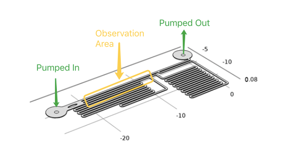
As the dimensions of the microfluidic devices are reduced, physics characteristics in conventional laboratory-scale is not applied. Usually the fluid flow in microfludic chips is laminar flow(Reynolds number<3). It leads to a drastic simplification of the complex Navier-Stokes equations describing fluid mechanics. For these reasons, dedicated microfluidic instruments have been designed to precisely control fluids inside microchannels. Each time when we applied a constant pumped inflow, cells in 3 different observation tunnel would receive corresponding small, middle, large, 3 level of force magnitude(around 1: 9: 81). By changing the pumped flow rate, we could measure MS channel response under a series of force with different magnitude order.
Syringe pump programmed by ourselves is a great tool for stimulation of accurate intensity and duration. In our experiment, the fluid flow will be maintained for about 2 min. And only after the cells have recovered from the last experiment (indicated by reverting to normal fluorescence intensity), would we start the next round of shear force stimulation.
During the experiment, the cells must tightly adhere to the channel bottom, by treating microfludics tunnel with gelatin, cell could adhere to the treated surface of glass slide. Once the cell have adhere to the glass slide, syringe pump was used to control the influx of medium to generate a shear stress on every channel walls. The fluorescence intensity of the cells would increased within a second by using R-GECO as an indicator of the intracellular calcium concentration. Live cell imaging system can capture its signal and record the data throughout whole experimental period, then, Matlab analysis was applied. For the cells which has a longer response time employing NFAT signal pathway, the change of gene expression(green fluorescent as downstream) can be observed under live cell imaging system after 20 hours.
Microfluidic chips in our experiment were made by polydimethylsiloxane (PDMS) fixed on a slide of glass. PDMS is the material for fast prototyping microfluidic devices. PDMS chips are widely used in laboratories, especially in the academic community due to their low cost and ease of fabrication. Here are listed the main advantages of such chips:
- Oxygen and gas permeability
- Optical transparency, robustness
- Non toxicity
- Biocompatibility
- No water permeability
One of the main drawbacks of PDMS chips is its hydrophobicity. Consequently, introducing aqueous solutions into the microchannels is difficult and hydrophobic analytes can adsorb onto the PDMS surface. Fortunately, there are now PDMS surface modification methods such as gas phase processing methods and wet chemical methods (or combination of both) to avoid issues due to hydrophobicity which we also employed in our experiment. After the fabrication of microfluidics channels having been done made by polydimethylsiloxane, they are treated with oxygen plasma for hydrophilic property. After this procedure, polydimethylsiloxane could bond to glass tightly.
How to fabricate
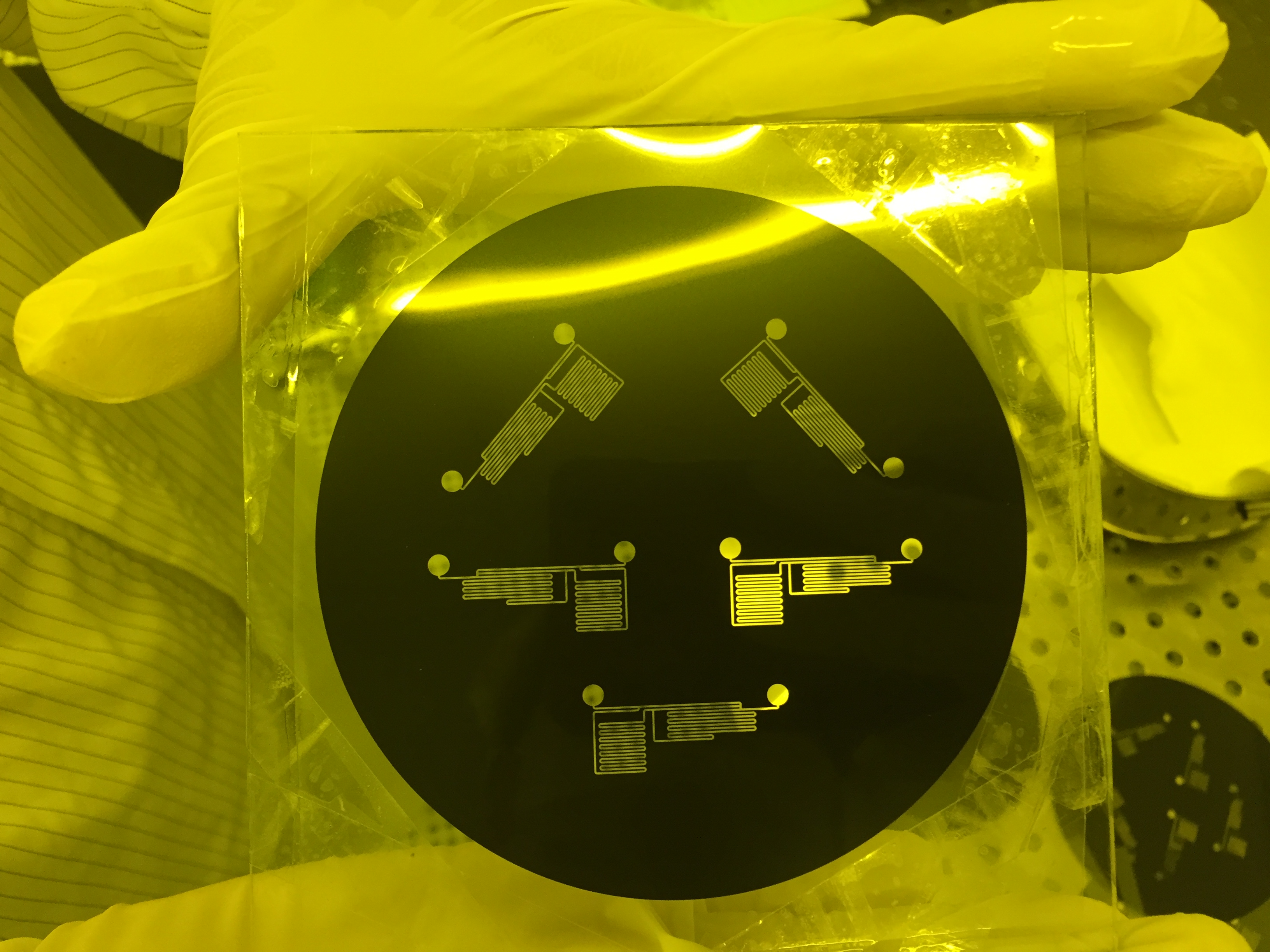
After reading existing papers about the processing technology typically used in microfluidic chips production and endless trial experiment, we have formed our own processing protocol based on our equipments and requirements.
The microfluidic chips used in our project were all produced using this protocol.
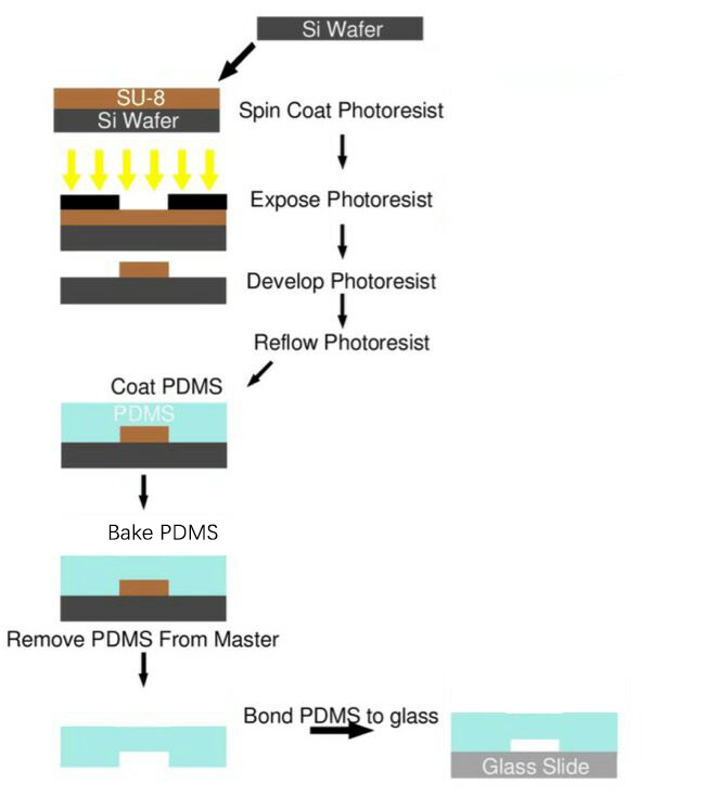
Process Overview
SU-8 Photoresist can cross-link to a network of polymer when exposed to short wavelength light. If the cross-linked network has formed, it cannot be dissolved by the SU-8 developer. So if we place a photo mask to shade the light shine on the photoresist, we can make a copy of the pattern on the photo mask.
Both PDMS and glass contains silicon element. When they were treated by oxygen plasma, unstable hydroxyl group will form on the treated surface. When they get close enough, two hydroxyl group will dehydrate and bond together covalently.


